Journal Information

Article Information


Original Paper

Analysis of Dispersion Characteristics of Rayleigh Waves in Nanostructured Thin Films

Tae-Sung Park[*], Yu-Min Choi[**], Byeong-Seok Cho[**], Ik-Keun Park[*][]

Abstract

The present study aims to theoretically analyze the dispersion characteristics of Rayleigh waves and verify the results through experiments. Raleigh waves are generated by scanning acoustic microscope, which are used to evaluate the thickness of thin films and the material characteristics of the samples. The transfer matrix method was used in the theoretical analysis of Rayleigh wave dispersion in thin films with slow-on-fast and fast-on-slow structures. To verify the dispersion diagram derived from the analysis, the e-beam evaporation and plasma-enhanced chemical vapor deposition technique was applied to fabricate slow-on-fast and fast-on-slow thin films of varying thicknesses. Slow-on-fast structures were created by depositing nickel (Ni) films on silicon (Si) substrates; fast-on-slow structures were produced by depositing silicon nitride (Si3N4) on gallium arsenide (GaAs) substrates. The scanning acoustic microscope used V(z) curves to precisely measure the velocity of the Rayleigh waves. This was to evaluate their dispersion depending on the thickness of each film. A comparison of the measured velocities against the theoretical dispersion diagram resulted in an error rate of less than 6% in the slow-on-fast structure and less than 10% in the fast-on-slow structure. In conclusion, this study confirmed that the theoretically derived dispersion characteristics correspond well with those observed in actual thin films, thereby suggesting the potential use of theoretical dispersion diagrams in evaluating the thickness and material characteristics of thin films.

Keywords: Scanning Acoustic Microscope, V(z) Curve, Rayleigh Wave, Dispersion Characteristics, Thin Films.


1. Introduction

Micro- and nanotechnologies have developed rapidly as leading technologies and a growth engine of the future through active research. Furthermore, these technologies play an important role as core technologies with enormous growth potential in modern science, engineering, and industries and have the potential to affect various industries such as the electronic, mechanical, chemical, communication, medical, energy, and optical industries.

Micro- and nanotechnologies refer to a series of technologies used to form films, such as insulators, conductors, and semiconductors, on a substrate using the mechanical, electrical, chemical, and optical characteristics of materials through various processes to produce specific patterns, structures, circuits, thin films, etc. Among them, thin films are used in electrical, chemical, optical, and mechanical applications as nonreflective and reflective coatings, interference filters, diffusion barriers, corrosion and oxidation prevention films, sensors, insulating and conductive films, and piezoelectric thin films [1-2].

To use thin films for specific applications, it is critical to precisely measure the thickness, composition, roughness, and other physical and optical properties of the thin film. In particular, the thickness of the thin film should be accurately measured because it is one of the factors that considerably affects the physical properties of the thin film [3].

Currently, typical methods for measuring the thickness of metal thin films include using a surface profiler like an atomic force microscope (AFM) or a scanning electron microscope (SEM). However, the surface profiler measures the difference between the portion having a thin film and that without a thin film after forming a step by attaching an insulating polyamide (PI) tape to a specimen, and it is difficult to measure the thickness if it is difficult to form a step or the surface of the substrate is not flat. Furthermore, the SEM method is a destructive method that does not allow reuse of a thin film because the film is deposited on the substrate and its thickness is measured by cutting the specimen and observing the cross section.

For this reason, studies have recently been conducted to nondestructively measure the thickness of a thin film using a scanning acoustic microscope.

Park et al. [3] attempted to measure the thickness of a thin film using the change in ultrasonic velocity according to the thickness of the thin film. However, this study only confirmed the tendency of velocity changes according to the thickness of the thin film. To quantitatively measure the thickness of a thin film using a scanning acoustic microscope, it is necessary to theoretically calculate the change in the velocity depending on the type of thin film and substrate, its dispersion curve [4,5]. Therefore, in this study, the dispersion characteristics of Rayleigh waves are theoretically analyzed according to the type of thin film and substrate, and the theoretical results are compared with the experimental results.

2. Theory

2.1 Multilayered thin film structure

The structures of thin films range from single thin film structures to laminated structures like semiconductors. Most thin films have multilayered structures with a finite number of layers above a substrate, as shown in Fig. 1. Thin films having a multilayered structure that generates different acoustic characteristics depending on the material constituting each layer. In Fig. 1, P and S denote upward longitudinal and transverse wave components, and P′ and S′ denote downward longitudinal and transverse wave components. Because each layer has different physical properties, it affects the propagation of Rayleigh waves and shows different propagation characteristics depending on the shape of the thin film structure. Typical examples are slow-on-fast and fast-on-slow thin film structures. The former refers to the case where the acoustic wave speed in the substrate is faster than the acoustic wave speed in the thin film, and the latter refers to the opposite case. These two thin film structures have opposite dispersion characteristics. In this study, the dispersion characteristics were calculated and experimentally verified by considering both slow-on-fast and fact-on-slow thin film structures.

Fig. 1

Schematic diagram of the multi-layered thin film structure

2.1 Dispersion curve in a multilayered structure

As mentioned above, because Rayleigh waves have velocity dispersion in a multilayered structure, the dispersion characteristics according to the frequency and thin film thickness were analyzed through a dispersion diagram using the transfer matrix method [6,7].

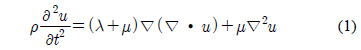
The displacement can be expressed in vector form through an analysis of the three-dimensional wave equation as follows [8]:

where u is the displacement vector in the x, y, or z directions, λ and μ are the Lame’s constants of the material, and ρ is the density of the material. The solutions to Eq. (1) can be divided into equations for longitudinal and transverse waves, respectively. If the above equation is expressed 
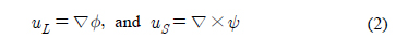
by the scalar function ϕ and vector ψ function by the Helmholtz equation, the following equation is obtained [8]:

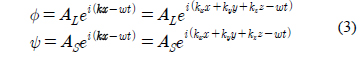
Furthermore, ϕ and ψ can be expressed as follows:

where k is the wavenumber vector, w is the angular frequency, and x and z are coordinates parallel and perpendicular to the surface, respectively, as shown in Fig. 1. It is assumed that the component in the y direction does not exist because in Rayleigh waves, only the propagation direction 
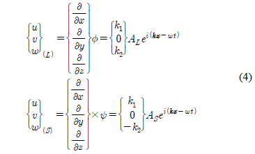
(x) and the depth direction (z) are considered. Eqs. (1) and (3) can be rearranged with the displacement vectors for longitudinal and transverse waves as follows, where ux, uy and uz are the displacement vectors in the x, y, and z directions, respectively.

Bulk waves have the same components according to Snell’s law. The wavenumber vector 
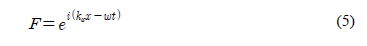
k is parallel to the medium. The equation for displacement and stress can be represented by F as follows:

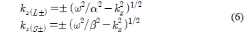
The wavenumber vector for the z direction is as follows, where α and β denote the sound velocities of longitudinal and transverse waves, respectively:

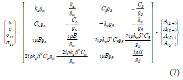
Eq. (6) can be substituted into Eq. (4), and the displacement and stress of the layer can be rearranged into an equation for the amplitude as follows by omitting the common component F [4]:

For each layer of the thin film, the downward direction is represented by + and the 
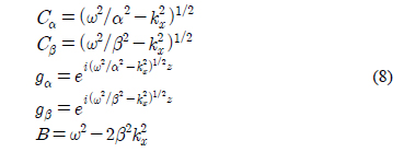
upward direction by −. In Eq. (7), Cα, Cβ, gα, gβ and B are random abbreviations for convenience and are defined as follows:

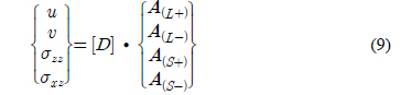
The 4×4 matrix in Eq. (7) can be used to define a coefficient matrix [D] and can be rewritten as follows:

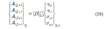
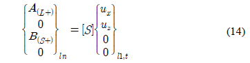
In a multilayered structure of the type shown in Fig. 1, the amplitude vector of the top layer can be expressed as the inverse matrix of the coefficient matrix [D] as follows:

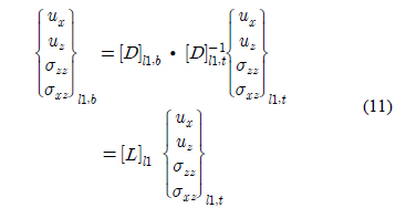
where the subscript l1 denotes the layer of the sequence, and t denotes the top layer. The relational equation for the top and bottom of the first layer can be expressed as follows:

where the matrix [L] is a coefficient matrix representing the relationship between the top and bottom 
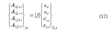
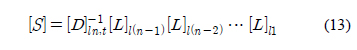
interfaces of a layer. Assuming that the index of the last layer is n, the relationship between the surface the bottom layer is defined as follows:

where matrix [S] is

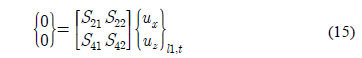
In order to solve Eq. (12), the boundary condition for Rayleigh waves must be applied. The stress components σzz and σxz at the top of the first layer are zero because according to the free stress condition. As there are no longitudinal and transverse wave components reflected from the half-space, the amplitude vectors A(L-) and B(S-) are zero. Therefore, the equation for a semiinfinite substrate in free space can be expressed as follows:

The 0 items in the left term can be removed and rearranged as follows:

For the above equation to be valid, the determinant of matrix [S] must equal 0. This is known as the characteristic equation of the Rayleigh wave.

The dispersion diagram is formed when the frequency and phase velocity satisfying the above characteristic equation are derived and expressed along the x and y axes, respectively.

2.3 Calculating V(z) curve and Rayleigh wave velocity

Fig. 2 illustrates the generation process of the V(z) curve between the acoustic lens of the scanning acoustic microscope and specimen.

Fig. 2

Schematic diagram of process for the V(z) curve measurement

The RF input signal (tone burst mode) applies a voltage to a ZnO piezoelectric transducer through an electrode. The transducer propagates the plane acoustic wave through the buffer rod by the piezoelectric effect. When this acoustic wave propagates through a contact medium, specularly reflected acoustic waves and Rayleigh waves are generated. Rayleigh waves are generated when the incident waves with an angle greater than the critical angle propagate between the surface of the specimen and the contact medium due to the shape of the acoustic lens. After propagating for a certain distance along the interface, the Rayleigh waves leak into the contact medium layer before propagating again in the reverse direction.

The specularly reflected acoustic waves also propagate in the reverse direction after being reflected from the material surface and output a voltage owing to the inverse piezoelectric effect. If a tone burst wave is used, the output voltage changes periodically owing to the changing distance between the acoustic lens and specimen caused by the interference of these two acoustic waves. The V(z) curve graphically represents this relationship and can be used to calculate the propagation velocity of Rayleigh waves. This velocity is calculated using the interval (Δz) between the valleys in the interval where the periodic voltage changes occur in the V(z) curve, and is calculated using Eq. (17), where VR is the velocity of the Rayleigh waves, and vw is the acoustic wave velocity in water.

3. Specimen fabrication and experimental method

3.1 Fabricating thin film specimens

Slow-on-fast and fast-on-slow thin film specimens were fabricated to evaluate the dispersion characteristics. The slow-on-fast structure consists of an Ni thin film deposited on an Si substrate using e-beam evaporation. A 6-inch Si wafer was used as the substrate of the Ni/Si thin film. Before deposition, ultrasonic cleaning was performed with alcohol, acetone, and distilled water, in that order. Then the surface was fully dried with nitrogen gas. To verify the dispersion characteristics according to the specimen thickness, specimens were fabricated by controlling the deposition time and the thin film thickness after calculating the deposition rate through preliminary deposition. Ni thin films with thicknesses of 100, 200, 400, 600, 800, and 1000 nm were deposited on the cleaned Si wafers. The fabricated specimens were diced to a size of 1 cm × 1 cm to measure the velocity of Rayleigh waves and the actual deposited thickness using a SEM. For the fast-on-slow structure, Si3N4 was deposited on a GaAs substrate using plasma-enhanced chemical vapor deposition (PECVD).

A 2-inch GaAs substrate and mixed gas of 5% silane/helium (SiH4/He) and ammonia (NH3) were used to fabricate an Si3N4/GaAs thin film, where the chamber temperature was maintained at 250℃ during deposition. Furthermore, the deposition rate was calculated and the deposition time was controlled through preliminary deposition in the same manner as for the Ni/Si thin-film fabrication process. The resulting Si3N4/GaAs thin-film specimens had thicknesses of 100, 400, 800, 1200, 1600, and 2000 nm. For the two types of fabricated specimens, the actual thickness was accurately measured using an SEM. Figs. 3 and 4 show the cross-sectional images of the thin films measured using an SEM, and Tables 1 and 2 show the measured thicknesses of the thin films.

Fig. 3

Cross-sectional image of Ni/Si thin film

Fig. 4

Cross-sectional image of Si3N4/GaAs thin film

Thickness of Ni thin film [unit: nm]

100 200 400 600 800 1000
1 135.0 217.5 303.7 472.5 731.2 946.9
2 129.4 217.5 318.7 476.2 750.0 960.0
3 131.2 215.6 311.2 457.5 751.9 946.9
Avg. 131.8 216.8 311.2 486.7 744.3 951.2

Thickness of Si3N4 thin film [unit: nm]

100 400 800 1200 1600 2000
1 87.5 328.1 768.8 1046.9 1506.3 1812.5
2 90.6 326.1 762.5 1056.3 1493.8 1815.3
3 90.6 328.1 765.6 1059.4 1053.1 1812.5
Avg. 89.6 327.4 765.6 1,054.2 1,501.1 1,813.4

3.2 Measuring velocity of Rayleigh waves

To theoretically calculate and experimentally verify the dispersion characteristics of Rayleigh waves in this study, the acoustic velocity of Rayleigh waves in the thin films was determined by measuring the V(z) curve with a scanning acoustic microscope (Olympus; UH3).

In line with the section describing the velocity dispersion of Rayleigh waves, spherical probes with operating frequencies of 400 MHz and 200 MHz were used for the Ni and Si3N4 thin films, respectively. Probes with a 120° lens angular aperture were used to generate Rayleigh waves. Deionized water was used as the contact medium between the specimen and lens. The temperature was maintained at 21.5 ℃ using a heater in the sample stage to attempt to maintain a constant propagation velocity, regardless of the temperature of the contact medium. The velocity was measured in each specimen three times at random positions, and the velocity of the Rayleigh waves was calculated using the average value.

4. Results and Discussion

In this study, the dispersion characteristics of Rayleigh waves were theoretically analyzed according to the types of thin films and substrate, and compared with the experimental results. For this purpose, two types of thin film specimens, slow-on-fast and fast-on-slow, were fabricated at different thicknesses, and the dispersion curves for these specimens were theoretically calculated and experimentally verified. Figs. 5 and 6 show the theoretical dispersion diagrams for Rayleigh waves in the fabricated Ni/Si and Si3N4/GaAs thin films to simulate the slow-on-fast and fast-on-slow structures, respectively. The slow-on-fast thin film in Fig. 5 shows positive dispersion, where the velocity of Rayleigh waves (R1 mode) decreases as the frequency and thickness of the specimen increase.

Fig. 5

Dispersion curves of leaky surface acoustic wave for the Ni/Si thin film structure

Theoretically, higher-order modes such as S1 and S2 are generated. In reality, however, only Rayleigh waves are generated and propagate along the surface of the thin film when the scanning acoustic microscope is used. Theoretically, on the other hand, the velocity of Rayleigh waves tends to increase as the frequency and thickness of the thin film thickness increase, and no higher-order mode is generated in the fast-on-slow structure shown in Fig. 6. To experimentally verify the dispersion according to the thickness of these two types of thin films, the velocity of the Rayleigh waves in the thin films was accurately measured using the V(z) curve method with the scanning acoustic microscope.

Fig. 6

Dispersion curves of leaky surface acoustic wave for the Si3N4/GaAs thin film structure

Tables 3 and 4 list the velocities of Rayleigh waves measured in each type of thin-film specimen. To compare with the theoretically calculated dispersion diagram, the measured Rayleigh wave velocity is shown at the corresponding Frequency × Thickness value. In the case of the slow-on-fast structure, the velocity showed a decreasing trend as the thin-film thickness increased, as shown in Fig. 7, which matched well with the theoretical dispersion diagram. In addition, the velocities as a function of the thin-film thickness were determined through the theoretical and experimental dispersion diagrams, and the differences between these two values were verified as shown in Table 5. As a result, the error rate between the theoretical value and the experimental value was less than 6 %, confirming that they matched well. This result suggests that the theoretical dispersion diagram obtained in this study can be used to properly calculate dispersion in the slow-on-fast structure. Theoretically, the velocity tended to increase in the fast-on-slow thin film as the Frequency × Thickness value increased as described above. This confirms that the theoretical and experimental velocity dispersions match well. However, the fast-on-slow structure showed an error up to 10%, which is larger than that of the slow-on-fast structure. The reason for this seems to be the lack of accurate data regarding the phyical properties used in the theoretical calculation of the dispersion diagram, such as mass density and the longitudinal and transverse velocities.

Measured Rayleigh wave velocity of Ni/Si thin film [unit: nm]

100 200 400 600 800 1000
1 4,772 4,619 4,476 4,295 4,295 4,166
2 4,763 4,607 4,476 4,325 4,285 4,107
3 4,777 4,607 4,454 4,215 4,179 3,942
4 4,791 4,607 4,454 4,215 4,161 3,935
5 4,777 4,595 4,465 4,285 4,143 3,912
Avg. 4,776 4,607 4,465 4,267 4,212 4,012

Measured Rayleigh wave velocity of Si3N4/GaAs thin film [unit: nm]

100 400 800 1200 1600 2000
1 2,714 2,862 3,051 3,126 3,134 3,182
2 2,745 2,880 3,044 3,142 3,165 3,190
3 2,740 2,862 3,051 3,126 3,157 3,190
4 2,745 2,862 3,044 3,118 3,173 3,190
5 2,745 2,868 3,037 3,126 3,182 3,190
Avg. 2,738 2,867 3,045 3,128 3,162 3,188

Fig. 7

Theoretical and experimental Dispersion characteristic of Rayleigh wave for the Ni/Si thin film structure

Fig. 8

Dispersion curves of Rayleigh wave for the Si3N4/GaAs thin film structure

Comparison of theoretical and experimental Rayleigh wave velocity on Si/Ni thin films

100 200 400 600 800 1000
Calculated velocity [m/s] 4,885 4,723 4,557 4,290 3,985 3,794
measured velocity [m/s] 4,776 4,607 4,465 4,267 4,212 4,012
Relative error [%] 2.3 2.5 2.1 0.5 5.4 5.4

Comparison of theoretical and experimental Rayleigh wave velocity on Si3N4/GaAs thin films

100 200 400 600 800 1000
Calculated velocity [m/s] 2,999 3,133 3,229 3,279 3,320 3,339
measured velocity [m/s] 2,738 2,869 3,045 3,128 3,162 3,188
Relative error [%] 9.5 9.3 6.0 4.8 5.0 4.7

5. Conclusions

This study theoretically calculated and experimentally verified the dispersion characteristics of Rayleigh waves in nanoscale thin films. To that end, dispersion diagrams in the slow-on-fast and fast-on-slow structures were derived using the transfer matrix method. The result theoretically confirmed that a higher-order mode was generated in the slow-on-fast structure with positive dispersion. In contrast, the fast-on-slow structure showed abnormal dispersion and did not generate a higher-order mode. To experimentally verify these results, slow-on-fast and fast-on-slow structures were fabricated, and their dispersion characteristics were verified by controlling the thin-film thickness and were compared with the theoretical dispersion diagram. The results from the slow-on-fast structure had an error of less than 6 %, whereas the results from the fast-on-slow structure had up to 10 % error. These errors seem to be caused by the difference between the physical properties appearing in the transfer matrix and thin film used to obtain the dispersion diagram. These errors will decrease if accurate physical properties are used. In conclusion, the results in this study confirmed the possibility of estimating the thickness and other physical properties of thin films using the theoretical dispersion diagram derived in this study. In the future, this dispersion diagram can be improved to estimate the actual thickness and physical properties of thin films.

Acknowledgements

This study was supported by the Research Program funded by the SeoulTech(Seoul National University of Science and Technology)

References

[1]

H. S. Ju and B. R. Tittmann, "Recent advances in scanning acoustic microscopy for adhesion evaluation of thin films," Journal of the Korean Society for Nondestructive Testing, Vol. 29, No. 6, pp. 534-549 (2009)

[2]

V. Natarajan, "Micro and nano science and technology: naval perspective," Science Spectrum, Defence Research & Development Organization, pp. 237-244 (2009)

[3]

T. S. Park and D. R. Kwak, I. K. Park, M. Kim. S. S. Lee, "Thickness measurement of ni thin film using dispersion characteristics of a surface acoustic wave," Journal of the Korean Society for Nondestructive Testing, Vol. 34, No. 2, pp. 171-175 (2014) [CrossRef]

[4]

M. J. S. Lowe, "Matrix techniques for modeling ultrasonic waves in multilayered media," IEEE transactions on ultrasonics, ferroelectrics, and frequency control, Vol. 42, No. 4, pp. 525-542 (1995) [CrossRef]

[5]

M. Kim, S. H. Cho, G. W. Jang, S. S. lee, I. K, Park, "Investigation on guided wave dispersion characteristics for metal thin films," Journal of the Korean Society for Nondestructive Testing, Vol. 34, No. 3, pp. 233-240 (2014) [CrossRef]

[6]

W. T. Thomson, "Transmission of elastic waves through a stratified solid medium," J. Applied Physics, Vol. 21, pp. 89-93 (1950) [CrossRef]

[7]

N. A. Haskell, "Dispersion of surface waves on multilayered media," Bulletin of the Seismological Society of America, Vol. 43, pp. 17-34 (1953)

[8]

L. E. Malvern, "Introduction to the mechanics of a continuous medium," Prentice-Hall Inc., Englewood New Jersey (1969)